
Design of Wireless Sensor Network Nodes Based on Microcontrollers and Wireless Communication Modules
This article introduces the design and implementation of a wireless sensor network node based on ATmega128L and CC2420 operating in the 2.4GHz frequency band, and discusses in detail the hardware composition of each part. Experiments have shown that nodes can flexibly form wireless sensor networks. The network system composed of nodes has stable performance, high communication efficiency, and low power consumption, and can be widely used in fields such as control, signal acquisition, and transmission.
Wireless sensor networks are an emerging research field with enormous potential applications in many fields such as military, environmental, health, home, and business. Wireless sensor network nodes are the basic units that make up a network. The rapid development of wireless sensor networks has posed many challenges to the design and management of wireless sensor network nodes.
Wireless sensor network nodes
Wireless sensor network is a distributed self-organizing network that integrates data collection, processing, and communication functions. A wireless sensor network is composed of multiple network nodes within a certain area that have wireless communication, sensing, and data processing functions. Sensor nodes are responsible for collecting, processing, compressing data, forwarding data packets from other nodes, and sending them out. In different applications, the structure of sensor network nodes varies and generally consists of data acquisition units (sensors, A/D converters), data processing and control units (microprocessors, memory), wireless communication units (wireless transceivers), and power supply units (batteries).
Compared to traditional wireless network nodes, wireless sensor network nodes have obvious technical characteristics: (1) high density and large number of network nodes; (2) The computing and storage capabilities of nodes are limited; (3) Nodes have a small volume and usually carry batteries with very limited energy, resulting in limited node energy; (4) The communication capability is limited, and the communication bandwidth of sensor networks is relatively narrow. The communication single hop distance between nodes is usually only a few tens to several hundred meters. Therefore, how to design a network communication mechanism to meet the communication needs of sensor networks under limited communication capability is a necessary issue to consider; (5) The positions of each sensor node are randomly distributed and have self-organizing characteristics.
Due to the above characteristics of wireless sensor network nodes, the design of nodes requires low hardware cost, low energy consumption, and support for multi hop routing protocols. The IEEE802.15.4/ZigBee protocol fully considers the requirements of wireless sensor network applications, and has the characteristics of device power-saving, communication reliability, network self-organization, strong self-healing ability, low cost, large network capacity, and network security. Based on these basic requirements, the hardware design of wireless sensor network nodes supporting the 802.15.4/ZigBee protocol has been carried out.
network structure
Nodes can form three topological structures: star structure, mesh structure, and cluster tree structure. Nodes form a self-organizing network, and each node can independently collect data. The data is sent to the aggregation node (Sink node) through single hop or multi hop relay methods. The aggregation node sends the collected data to a remote control center, or sends the data to a PC for data processing and storage through the RS232 interface.
Node design
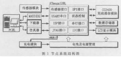
The node hardware adopts a modular structure design, as shown in Figure 1, consisting of a computing and communication sub board, a sensor sub board, and a charging and status display sub board. The computation and communication sub board consists of a microprocessor, data storage circuit, wireless communication module, power management module, etc. Its main function is to store and process data, complete wireless communication between nodes, and provide energy to the system. The sensor sub board consists of several sensors responsible for collecting information within the monitoring area. The charging and status display sub board consists of a charging module and an LCD display module, which is used to display the charging status of the node battery, the working status of the node, and the battery level.
Microprocessor circuit
The microprocessor circuit adopts Atmel's ATmega128L microcontroller, which is produced using low-power CMOS technology and is based on RISC structure. It has 128KB on-chip program memory (Flash), 4KB data memory (SRAM), and 4KB EEPROM. It has 8 10 bit ADC channels, 2 8-bit and 2 16 bit hardware timing/counters, 8 PWM channels, programmable watchdog timer and on-chip oscillator, on-chip analog comparator, JTAG, UART, SPI I2C bus and other interfaces. The ATmega128L can operate in multiple different modes, and in addition to the normal operation mode, it also has six different levels of low-energy operation modes, making it suitable for low-energy applications. The interface diagram is shown in Figure 2.
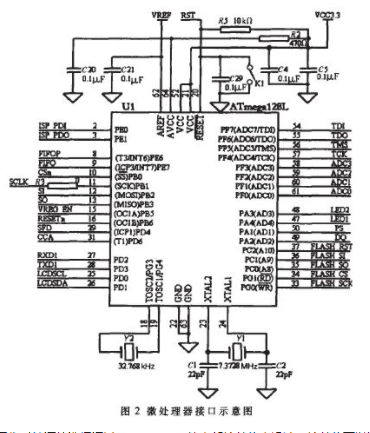
The working clock source of ATmega128L can be selected from external crystal oscillator, external RC oscillator, internal RC oscillator, external clock source, etc. The selection of the working clock source is designed through the internal fuse position of ATmega128L, which can be set through JTAG programming, ISP programming, and other methods. In this design, ATmega128L uses two external crystal oscillators: a 7.3728MHz crystal oscillator as the working clock of ATmega128L; 32.768kHz crystal oscillator as a real-time clock source.
Data storage circuit
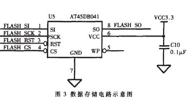
Due to the limited transmission capacity of the communication module of wireless sensor nodes and the very small duty cycle of node operation, many data cannot be forwarded in real time. Therefore, a manageable memory is needed to store this data, temporarily storing the data collected by oneself or other nodes that need to be forwarded. This design uses 512KB serial FLASHAT45DB041 to store data. Compared with ordinary data memory, this chip has the characteristics of low power consumption, small size, serial interface, and simple external circuits, making it suitable for use in sensor nodes. The schematic diagram of the data storage circuit is shown in Figure 3.
Wireless communication module
The wireless communication module adopts the wireless RF CC2420 module. It is a wireless transceiver module compatible with the 2.4GHz IEEE802.15.4 standard launched by Chipcon at the end of 2003. Based on Chipcon's SmartRF03 technology, it is produced using CMOS technology, with low operating voltage, low energy consumption, small size, and programmable output strength and transceiver frequency. This chip only requires a few external components such as a crystal oscillator, load capacitor, input/output matching element, and power decoupling capacitor to operate normally, ensuring the effectiveness and reliability of short distance communication. Its maximum transmission and reception speed is 250kbps.
CC2420 has 33 16 bit configuration registers, 15 command gating registers, 1 128 byte transmit FIFO buffer, 1 128 byte receive FIFO buffer, and 1 112 byte security information storage. The connection between CC2420 and the processor is relatively simple. It uses four pins, SFD, FIFO, FIFOP, and CCA, to indicate the status of transmitting and receiving data; The processor exchanges data and sends commands with CC2420 through SPI interfaces (CSn, SO, SI, SCLK), uses RESETn pins to reset the chip, and uses VREG_ The EN pin enables the voltage regulator of CC2420 to generate the required 1.8V voltage for CC2420, thereby enabling CC2420 to enter a normal working state; CC2420 communicates through a monopole antenna or PCB antenna. The schematic diagram of its module is shown in Figure 4.
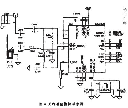
CC2420 requires a 16MHz reference clock for data transmission and reception. The reference clock can come from an external clock source or be generated by an internal crystal oscillator. If using an external clock, directly from XOSC16_ Q1 pin input, XOSC16_ Q2 foot suspended; If using an internal crystal oscillator, the crystal oscillator is connected to XOSC16_ Q1, XOSC16_ Between Q2 pins. The crystal oscillator needs to be activated by enabling the CC2420 gating command register SXOSCON.
Power management module
Electricity is a very valuable resource for sensor networks. In order to ensure low-power design of hardware circuits, low-power and low-voltage chips are used for node chip selection. The system operates with regular batteries or rechargeable lithium-ion batteries, and the power management chip is packaged in AD company's ADP3338-3.3. SOT-223.
Charging and status display module
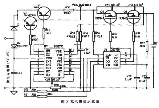
When conditions permit charging of a node, the node operates with a lithium-ion battery. The charging module can be used to supplement the node's electrical energy, ensuring the continuity of the node's operation and avoiding work interruptions caused by battery replacement. The charging module is designed using Dallas DS2770 and battery protection chip DS2720, and has functions such as charging control, power control, battery counting, and battery protection. The processor and DS2770 use a one line interface to transmit information and require an external connection of approximately 4.7k! Pull up resistance of. The schematic diagram of the charging module is shown in Figure 5. The LCD display module adopts an LCM6432ZK LCD display, which is connected to the main MCU through a serial interface and is used to display the system's working status information, charging process, battery level, and other status. The node hardware has an LCD interface, which allows for easy insertion of LCD display modules when needed for display.
Sensor module
The node sensor module is separated from the computing and communication sub boards, and the modular design improves the flexibility of the node in different applications. The sensor module can determine suitable sensors according to actual needs, such as temperature, humidity, vibration, light intensity, gas alarm, magnetic resistance, infrared, etc., to meet different needs. Due to the fact that most nodes are powered by batteries, it is recommended to use digital sensors that do not require complex signal conditioning circuits, as they require small sensor size, low power consumption, and simple peripheral circuits.
The selected sensors for this design are:
The temperature sensor DS18B20 is a new type of digital temperature sensor, with a very simple external circuit and a one wire bus interface. Its measurement range is -55 ℃ to 125 ℃, with a measurement accuracy of ± 0.5 ℃ between -10 ℃ to 85 ℃. The maximum resolution can be designed to 12 bits, and the measurement data is accurate and reliable.
The PD632 infrared sensor is a digital pyroelectric sensor with a working wavelength of 7.5 η M-14 η m. The detection distance can reach 6-15m in a working environment of -20 ℃ to 60 ℃.
The ADXL202 accelerometer is a two-dimensional digital accelerometer from AD company, operating at temperatures ranging from -40 ℃ to 85 ℃. It adopts advanced MEMS technology and can measure both vibration acceleration and static acceleration.
External interface
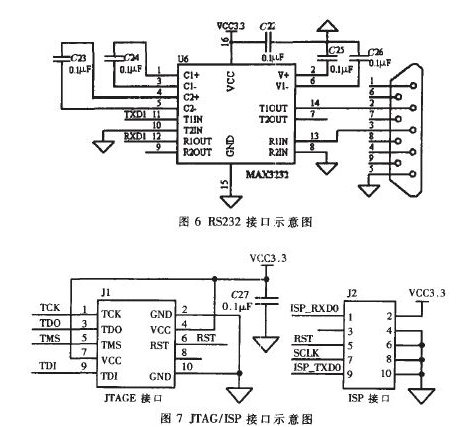
The external interfaces of the node include JTAGE interface, ISP programming interface, RS232 interface, charging interface, sensor interface, SMA antenna socket interface, etc. Nodes use various methods such as JTAGE and ISP to download programs; Connect directly to the PC serial port using the RS232 interface; Different sensor modules can be connected through sensor interfaces according to different needs; Under charging conditions, the node can be quickly replenished with energy through the charging interface. Figure 6 is a schematic diagram of the RS232 interface, and Figure 7 is a schematic diagram of the JTAG/ISP interface.
Key points and precautions in node design
The RF part is the focus and difficulty of this design, and it is also the key to the successful system design. The main problems encountered during the module design process and their solutions include:
The carrier frequency of CC2420 is 2.4GHz, with an additional channel every 5MHz. The accuracy of the crystal oscillator will affect the frequency of the carrier, thereby affecting the establishment and stability of communication. CC2420 requires the accuracy of the clock source to be within ± 40ppm. If using an external crystal oscillator, try to use a four pin SMT crystal oscillator with high accuracy and stable performance.
The CC2420 RF circuit operates in the high-frequency operating frequency range of 2.400GHz to 2.4835GHz, and the anti-interference design directly affects the RF performance and the operation of the entire sensor node. Reasonable layout and wiring, as well as the use of multi-layer boards, are both necessary and effective means to reduce electromagnetic interference and improve anti-interference ability when wiring in the RF section. When wiring, special attention should be paid to the following points: firstly, the area of the RF circuit that is not used for wiring needs to be filled with copper and connected to the ground to provide RF shielding and achieve effective anti-interference; The second is that the bottom of the CC2420 chip should be grounded; To reduce latency, reduce crosstalk, and ensure the transmission of high-frequency signals, multiple grounding vias should be used to connect the bottom of the CC2420 chip to the ground layer; The third is to minimize crosstalk and minimize the influence of distributed parameters. The devices should be tightly distributed around CC2420 and smaller packaging should be used.
For wireless communication networks, antennas play a crucial role. The selection and setting of antennas will directly affect the operational quality of the entire wireless communication network. The CC2420 RF chip at this node can use two design schemes: a metal inverted F-shaped PCB lead antenna and a monopole antenna. PCB lead antenna is a wire printed on a circuit board that senses airborne radio waves and receives information through it. The shape and size of PCB antennas should be strictly designed according to the data manual. In recent years, with the decrease in computer costs and the shrinking size of microprocessors, wireless sensor networks have received increasing attention. This design is a low-power, low-cost, and practical wireless sensor network node designed by the author based on summarizing the research achievements of wireless sensor networks at home and abroad. The node adopts independent optional charging modules, LCD status display modules, and rich external interfaces, which have strong practicality and can work in various environments. It can be configured according to various needs to complete system functions, and has obvious advantages in cost, power consumption, flexibility, and other aspects.