
Quantum semiconductor devices achieve topological skin effect, which can be used to manufacture micro high-precision sensors and amplifiers
Theoretical and experimental physicists from the CT. qmat team of the Werzburg Dresden Excellence Cluster in Germany have developed a semiconductor device made of aluminum gallium arsenic. This groundbreaking study was published in the latest issue of the journal Nature Physics.
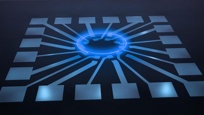
Quantum semiconductor devices that achieve topological skin effect, despite material deformation or other external disturbances, can still ensure unparalleled robustness with electrons flowing along the edges (blue circles). This quantum semiconductor marks a breakthrough in the development of micro topological electronic devices.
Due to the topological skin effect, all currents between different contacts on quantum semiconductors are not affected by impurities or other external disturbances. This makes topology devices increasingly attractive to the semiconductor industry, as they eliminate the requirement for material purity and the cost of material purification is extremely high. Topological quantum materials are renowned for their excellent robustness and are highly suitable for power intensive applications. The newly developed quantum semiconductor is both stable and highly accurate, making this rare combination an exciting new choice in sensor engineering.
New high-performance quantum devices can be manufactured using topological skin effect, and the size can also be made very small. The new topological quantum device has a diameter of approximately 0.1 millimeters and can be easily further reduced. The groundbreaking achievement of this achievement lies in the realization of microscale topological skin effect for the first time in semiconductor materials. This quantum phenomenon was first confirmed at the macroscopic level three years ago, but only in artificial metamaterials, not in natural metamaterials. Therefore, this is the first time that a highly robust and ultra sensitive micro semiconductor topological quantum device has been developed.
By creatively arranging materials and contacts on aluminum gallium arsenic semiconductor devices, the research team successfully induced topological effects under ultra-cold conditions and strong magnetic fields. They adopted a two-dimensional semiconductor structure, and the arrangement of the contacts can measure resistance at the edge of the contacts, directly displaying topological effects.
Researchers suggest that in new quantum devices, the current voltage relationship is protected by topological skin effect, as electrons are confined to the edges. Even if there are impurities in semiconductor materials, the current can remain stable. In addition, the contacts can even detect the slightest current or voltage fluctuations. This makes topological quantum devices very suitable for manufacturing high-precision sensors and amplifiers with extremely small dimensions.