
Intel achieves large-scale production of advanced 3D packaging technology
Intel announced that it has achieved large-scale production based on industry-leading semiconductor packaging solutions, including Intel's breakthrough 3D packaging technology Foveros, which provides flexible choices for multiple chip combinations, leading to better power consumption, performance, and cost optimization.
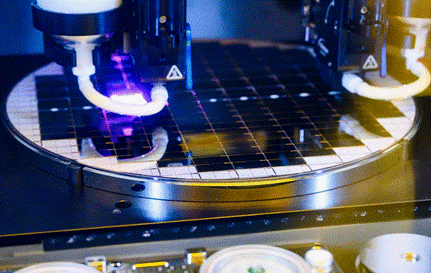
This technology was launched in the latest upgraded Fab 9 from New Mexico, USA. Keyvan Esfarjani, Executive Vice President and Chief Global Operations Officer of Intel, said, "Advanced packaging technology sets Intel apart, helping our customers gain competitive advantages in chip product performance, size, and flexibility in design applications."
This milestone progress will also drive Intel's next phase of advanced packaging technology innovation. As the entire semiconductor industry enters a heterogeneous era of integrating multiple "chips" in a single package, advanced packaging technologies such as Intel's Foveros and EMIB (Embedded Multi Chip Interconnection Bridge) provide a faster and cheaper path to integrate one trillion transistors in a single package, and continue to advance Moore's Law after 2030.
Intel's 3D advanced packaging technology Foveros is an industry-leading solution that allows computing modules to be stacked vertically rather than horizontally during processor manufacturing. In addition, Foveros enables Intel and its foundry customers to integrate different computing chips, optimize costs and energy efficiency.
Intel will continue to be committed to promoting technological innovation, expanding its business scale, and meeting the growing demand for semiconductors.